>> moving onto the speakers, bluetooth, and everything else.
this.. was the worst.

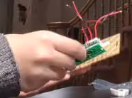
now that the PCB piece was done, it was time to attach everything else.
The kit provided a schematic of the PCB and how it connected to the external parts, and I also had to roughly build the plastic case it came with to see how everything could fit.
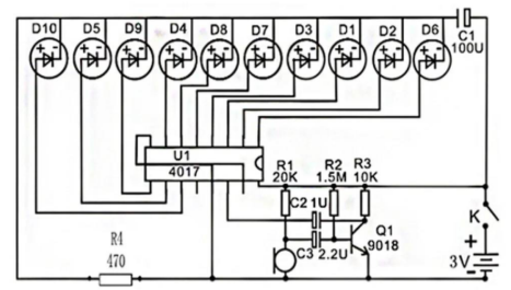
This was HELL for the electrically-illiterate Yvonne.
Just like a child who don’t know their left and rights, I didn’t know my negative and positive poles. I didn’t know where switch started and the USB cord (oh yeah there’s a US frickin B cord) ended. Don’t even get me started on the speakers and wires.
I was this close.

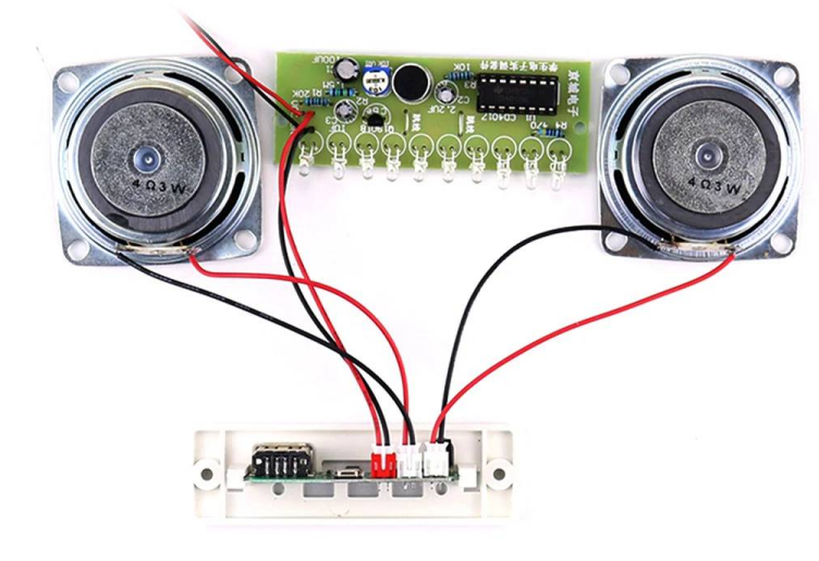
With much consulting with chatgpt, gemini, google, father, I managed to lay out everything properly according to the schematic:
- the speakers had to be soldered onto the jumper wires coming out of the Bluetooth
- the switch was connected to the USB cord and to the PCB board’s connectors.
This took much longer than it sounded. To test the switch’s polarity, I used a multimeter with the USB plugged into my computer to check when it turns on.
I also figured out much later the kit had an online file with the god-forsaken layout given already. (OH WELL. WE BALL I GUESS!?)

I had thought the first day was bad; this day took almost 6 hours.
TLDR; what did I learn?
- Find. An. Existing. Layout.
- Multimeters are your best friend.
- I need to read schematics.